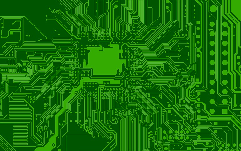
advantage of printed circuit board
advantage of printed circuit board
In past time, electronic component such as diode, triode, pentode, capacitor, resistor, etc, had be assembled on a metal base/ chassis for the manufacturer of various electronic device, such as radio, television, recorder, etc. The component have been connected together by single core insulated copper wire their wiring looks like network and their vacuum tube fitted on tube holder.
But, in present time, due to fast development in electronic field, complexity of the modern electronic equipment wiring have been very much increases. So for reducing the complexity of wiring. Printed circuit board (PCB) have been invented.
Advantage of PCB:-
1. During the time of assembled of any electronic equipment after inserting of electronic device such as resistance, diode, capacitor, and other components. There is no need for rechecking position of component, because for inserting above device or component, suitable places are already decided and their symbol have been printed on correct places and correct route of copper strips and layout already decided. So, there is no possibility of any mistake during assembled of electronic device and component on PCB.
2. High frequency circuit have been seperated from lower frequency circuit. So, that high frequency signals could not disturb the low frequency signals.
3. High voltage DC circuit have been seperated from low voltage circuit. So that high voltage lekage could not damage the low voltage component and device.
4. Soldering of electronic device and component pins with copper strips.
5. The length of the circuit is beings calculated already, according to load current width and thickness of circuit strips has been decided already. So that overheating of circuit strips could not be possible.
Construction of PCB:-
PCB works as base for electronic devices and component in electronics equipment, these base plates have been made of insulating material such as modern synthetic resin reinforced with paper, glass cloth or other fiberous material etc. The connection of electronic device and component, strips of thin copper sheet has been used on insulating base plate this copper stripes. So that connection pins can be soldered with copper strips circuit shape of layout of PCB. The symbol of electronic device have been printed already on suitable on back side of PCB. Hence, the component is soldered on suitable place which are decided already.
Material used for making base plate of PCB:-
Bakelite, phenolic resin reinforced with paper, or an epoxide resin reinforced with woven glass cloth and except these material modern synthetic resin reinforced with paper, glass, cloth or other fiberous material are mainly used in making of base plate of PCB.
Cutting and drilling operation are easily in insulating material. This insulating material have good insulating property and this material also bear heat during solding of electronic device and component pins with copper strips. The size of insulating material sheets are available in market is 1.2×0.9 m in 1mm to 2mm thickness which can be decided in required size with help of tennon savo.

